本文,我们给大家介绍基于思睿达主推的CR6267SJ 18W电源适配器方案。其中,IC集成了多种功能和保护特性,而且内置所有PIN脚悬空保护功能,使得芯片具有更高的可靠性。除了以上的特性以外,它的特点优势还不止这些,接下来就让我们一起来了解一下!
01、样机介绍
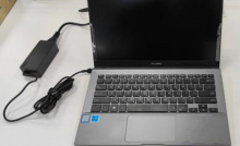
该测试报告是基于一个能适用于宽输入电压范围,输出功率18W,恒压恒流输出的电源适配器样机,控制IC采用了思睿达主推的CR6267SJ。
关于CR6267SJ
CR6267SJ是一款高性能原边检测控制的PWM 开关,待机功耗小于75mW。CR6267SJ内部采用了多模式控制的效率均衡技术,用于优化芯片系统待机功耗和提升效率,同时采用了初级电感量补偿技术和内部集成的输出线电压补偿技术,保证了芯片在批量生产过程中 CC/CV 输出精度,内置的全电压功率自适应补偿技术保证了系统在全电压范围(90V~264V)内输出恒定的功率。
CR6267SJ集成了多种功能和保护特性, 包括欠压锁定(UVLO),VDD 过压保护 (OVP),软启动,过温保护(OTP), 逐周期电流限制(OCP),CS 引脚悬空保 护,输出短路保护,内置前沿消隐电路, 输出整流二极管短路保护电路,输出过压护电路。而且内置所有PIN脚悬空保护功能,使得芯片具有更高的可靠性。
芯片特性
● CR6267SJ 内置650V 高压功率MOSFET,反激式原边检测PWM 功率开关;
● SOP8 封装,一侧引脚(5-8)全为内置MOS 漏极,方便散热设计;
● 内置软启动,减小MOSFET 的应力,内置斜坡补偿电路;
● 低功耗以及良好的负载动态特性;
● 具有良好的EMI 特性;
● 具有“软启动、OCP、SCP、OTP、OVP”等多种保护功能;
● 原边反馈,无需光耦和TL431,可调式线损补偿,IC 基准精度±1%;
● 电路结构简单、较少的外围元器件,适用于小功率AC/DC 电源适配器、充电器。
基本应用
● 小功率电源适配器
● 蜂窝电话充电器
● 数码电源充电器
● 电脑和服务器辅助电源
● 替代线性调整器和RCC
典型应用

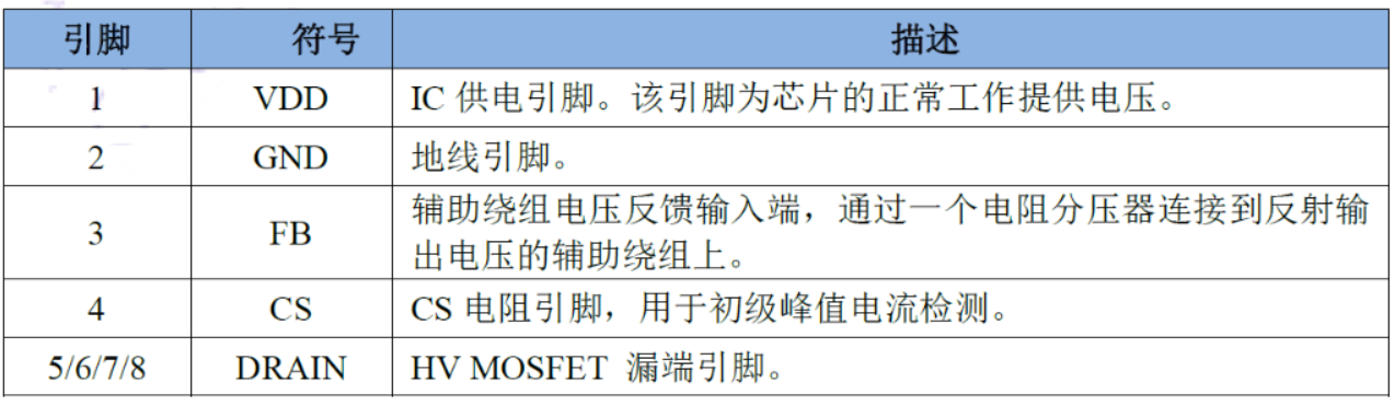
引脚分布
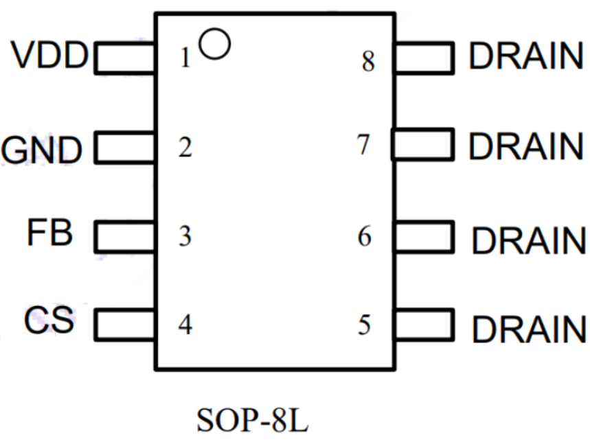
引脚描述
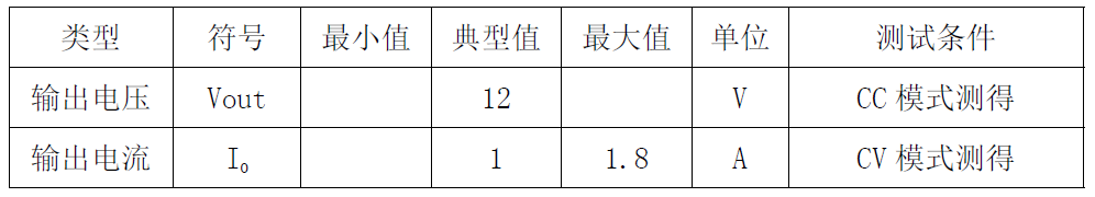
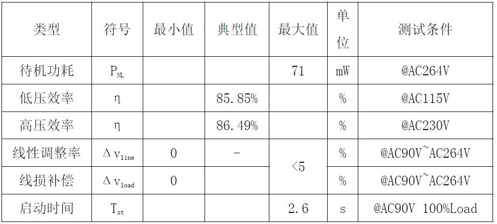
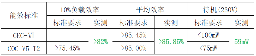
样机PCBA尺寸:66*39*21mm,是一款全电压实现12V1.5A输出的电源适配器。AC90V满足启动时间的条件下,实现AC264V样机待机功耗仅为71mW;同时效率能够满足最严格的“COC_V5_T2” 能效标准;全电压可实现±5%的CC/CV输出精度。
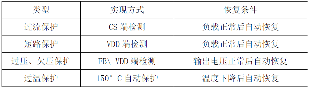
整机(含套件外壳)可满足40℃环境温度满载温升测试要求。样机具良好的恒流输出效果;同时具有“软启动、OCP、SCP、OVP、OTP自动恢复”等多种保护功能。
样机的变压器,采用了EE16W加宽磁芯(PC40材质)。变压器绕制工艺部分,请见后文详细说明。
02、样机特性
以下表格为工程样机的主要特性,具体测试方法在第4 章节中有详细说明。
2.1、输入特性:

2.2、输出特性(PCB END):
2.3、整机参数:
2.4、保护功能测试:
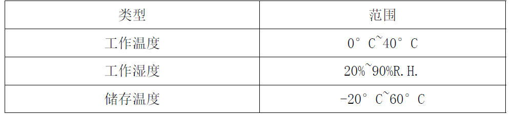
2.5、工作环境:
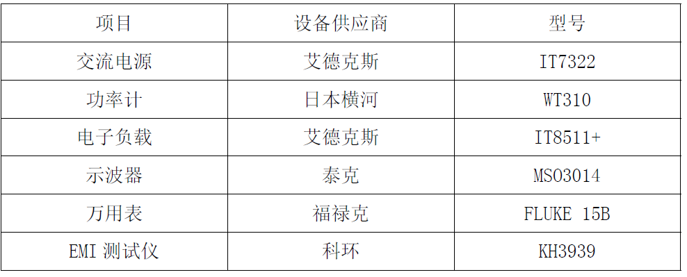
2.6、测试仪器:
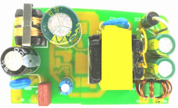
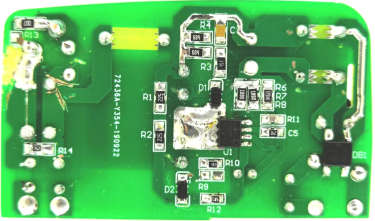
03、样机结构信息
本小节展示了工程样机的电路、版图结构,变压器结构及工艺。
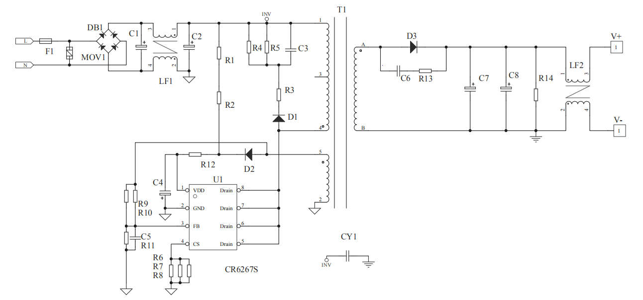
3.1、电路原理图及BOM:
3.1.1 原理图:
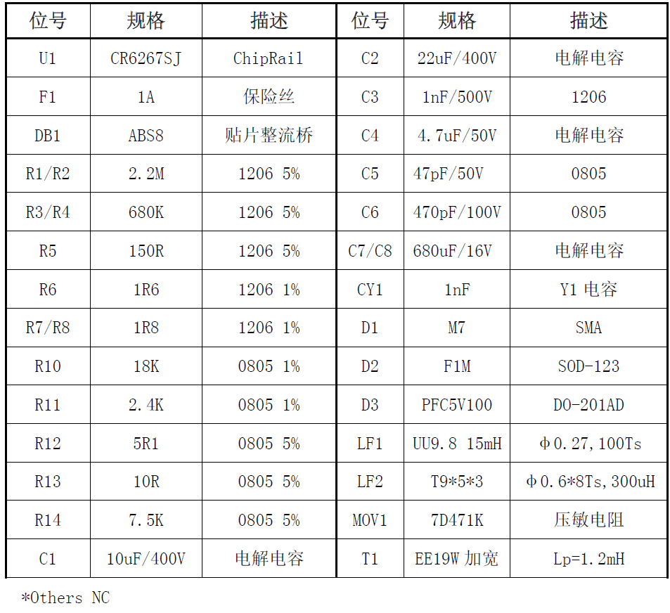
3.1.2、元器件清单:
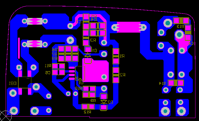
3.1.3、PCB 布局&布线:

3.2、变压器绕制工艺:
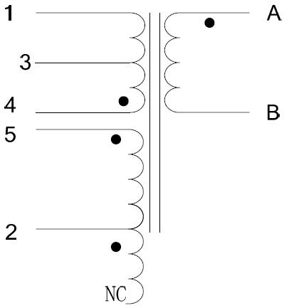
3.2.1、电路示意图:
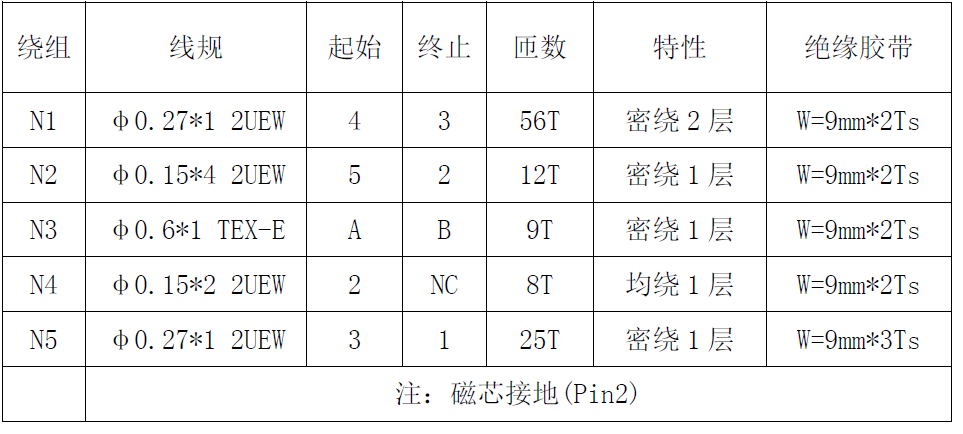
3.2.2、规格参数:
1)骨架:EE19W 加宽立式(5+5PIN),Ae=46mm²,槽宽8.5mm;
2)材质:TDK PC40 或同等材质;
3)N1、N2、N4、N5: 2UEW 漆包线;N3: 三层绝缘线;
4)次级绕组从变压器顶端进出线,磁芯接地
5)绝缘胶带:3M900 或同等材质;
6)初级绕组感量Lp:1200uH±5%(测试条件:0.3V,10kHz);
7)漏感量LLK:要求控制在初级绕组的5%以内(测试条件:0.3V,10kHz);
8)耐压测试= 3KV 5mA 1Min;
9)成品要求:浸凡立水;
3.2.3、变压器参数:
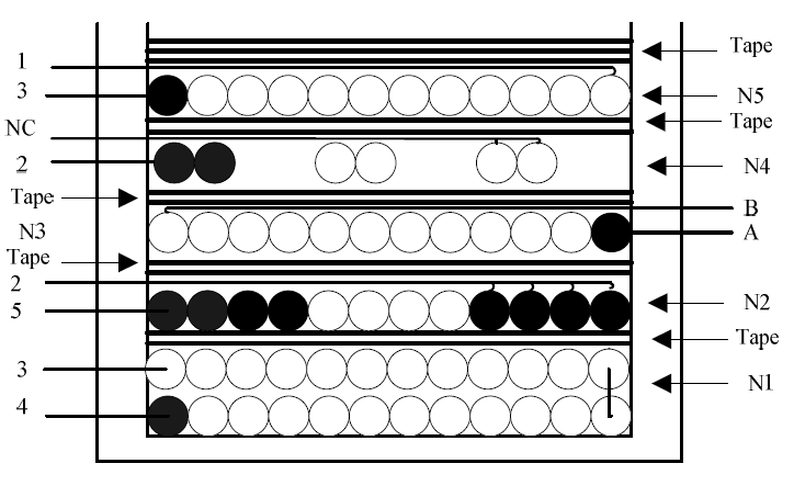
3.2.4、变压器结构示意图:
04、性能测评
本小节对工程样机的输入部分、输出部分、各种保护以及一些时序进行了测试,以下详解了测试方法及结果。从测试结果来看,以下各项测试均合格,能够满足大部分客户的要求。
4.1、输入特性:
本模板经过在不同的输入电压(从90V/60Hz 到264V/50Hz)和不同负载条件(空载和满载)下测试,得到待机功耗、效率及平均效率。
表1 待机功耗
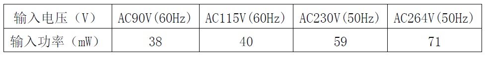
表2 输出100%负载下的输入特性
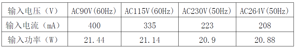
表3 效率测试(1.5m 22AWG Cable)

表4 效率测试(PCB END)
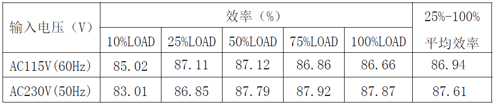
表4 能效等级评估(1.5m 22AWG Cable)
4.2、输出特性:
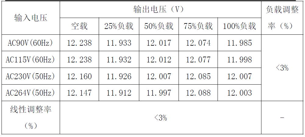
4.2.1、线性调整率和负载调整率: (1.5m 22AWG Cable)
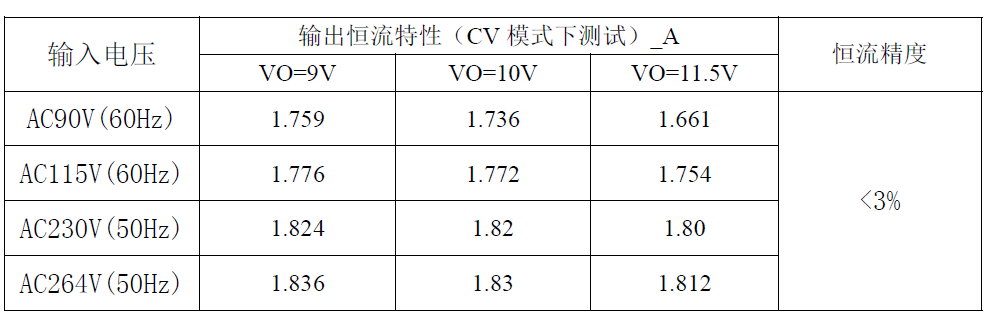
4.2.2、输出恒流特性:
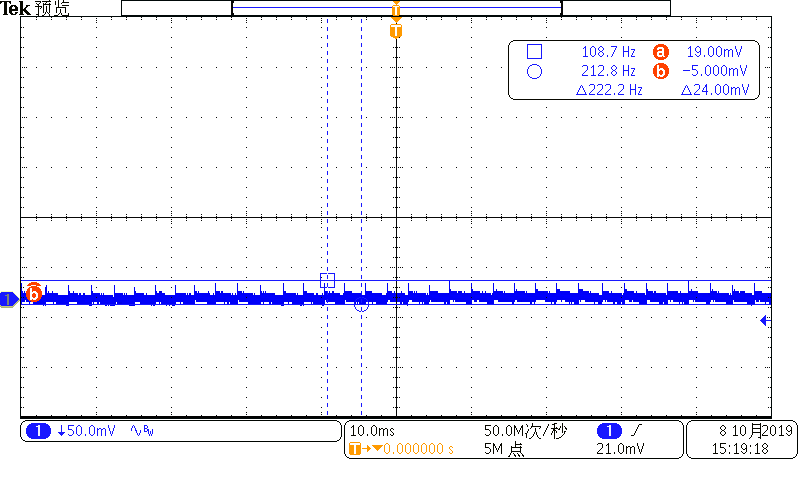
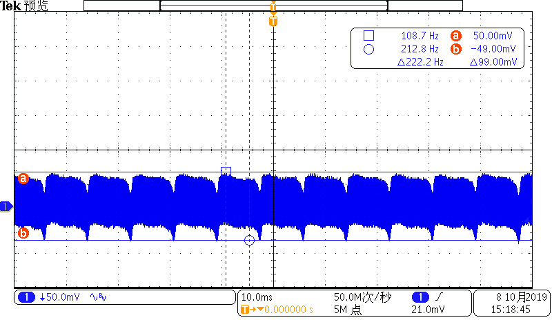
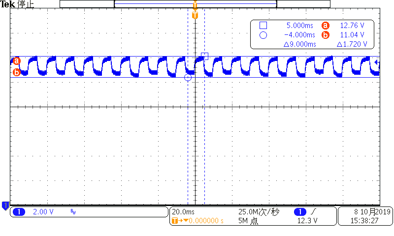
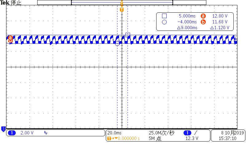
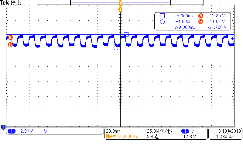
4.2.3、输出电压纹波:
注:纹波及噪声在1.5m 22AWG 处测试,测试端并联0.1uF/50V 的瓷片电容和10uF/50V 电解电容,带宽限制为20MHz。

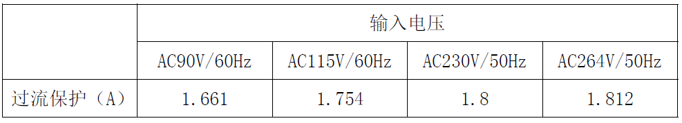
4.3、保护功能:
以下涉及过流保护、短路保护的测试。
4.3.1、过流保护及恒流特性
4.3.2、短路保护:
功率计电流量程2.5A,开启平均值模式测量。

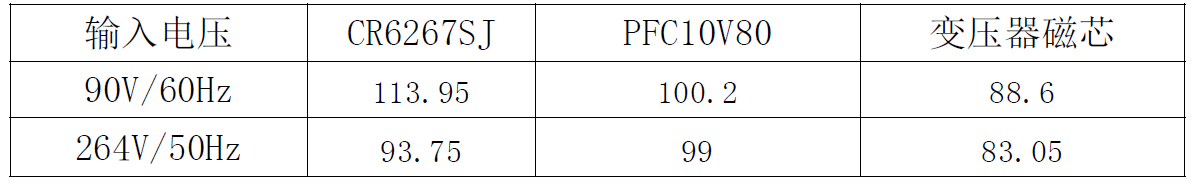
4.4、系统温升测试
本项测试评估成品样机(含配套塑料外壳)在40℃环境温度下长时间工作时关键器件的稳态温度值。测试条件:输入电压分别为90V~264V,输出电流1.5A。

温升测试(℃):
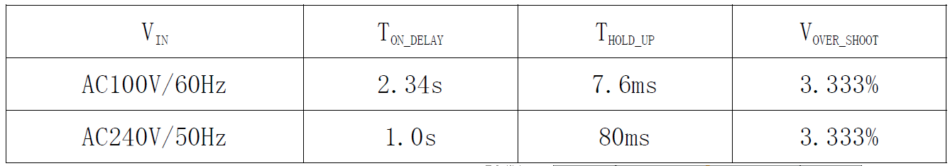
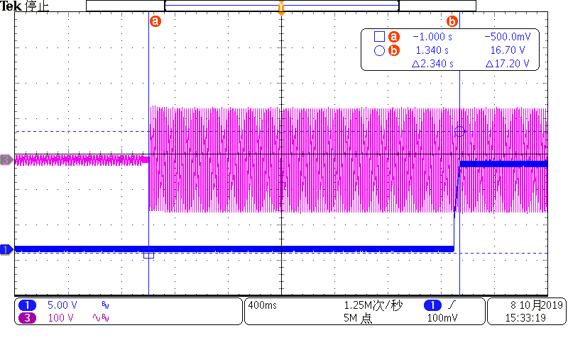
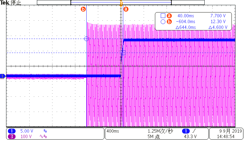
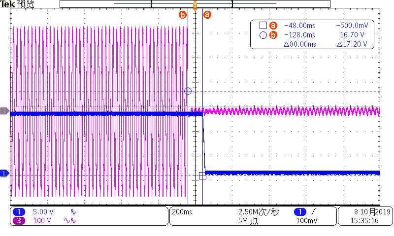
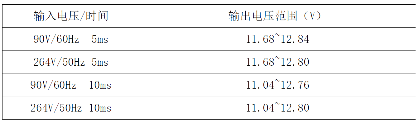
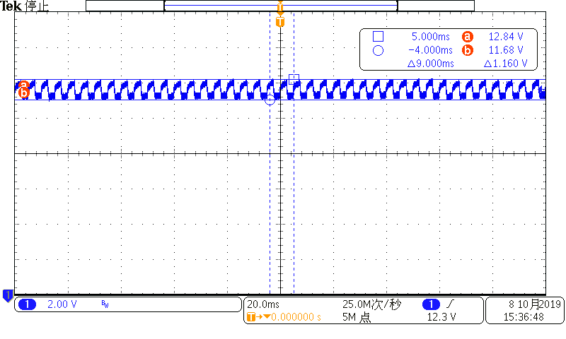
4.5、系统延时时间测试:

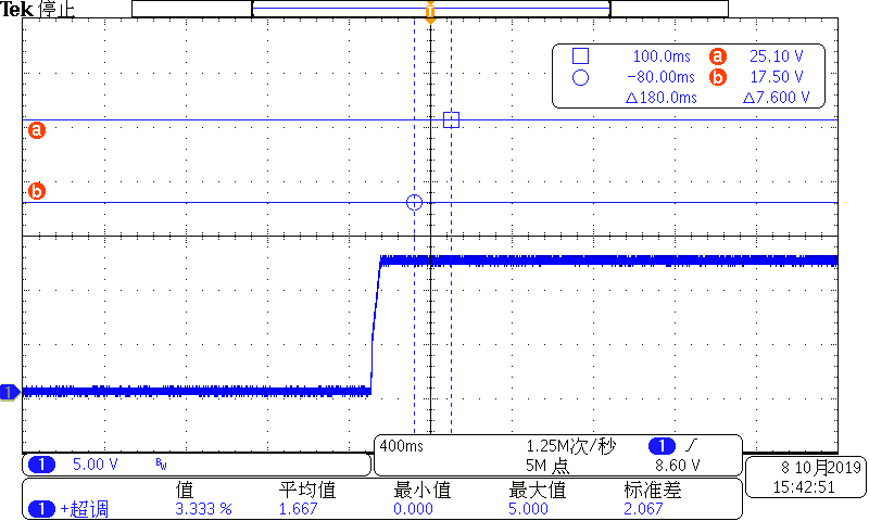
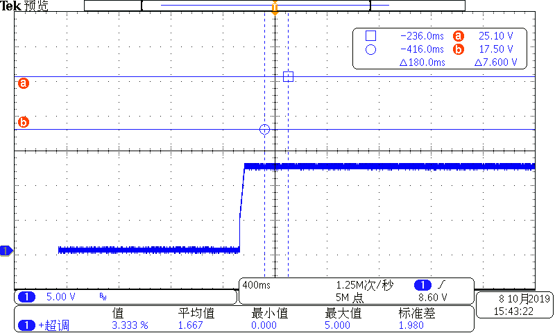
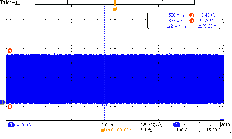
4.6、动态测试:
注:输出动态负载电流设置为1.5A 持续5/10ms,然后为0A 持续5/10ms 并持续循环,上升/下降设置为3A/us。
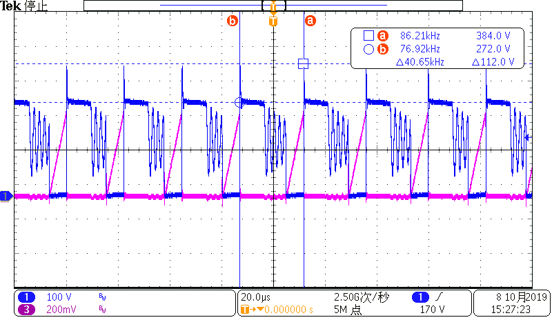
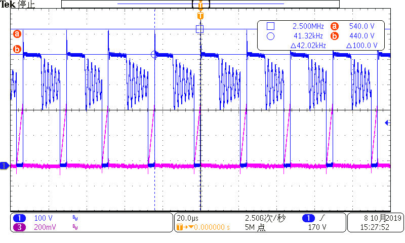
4.7、其它重要波形测试:
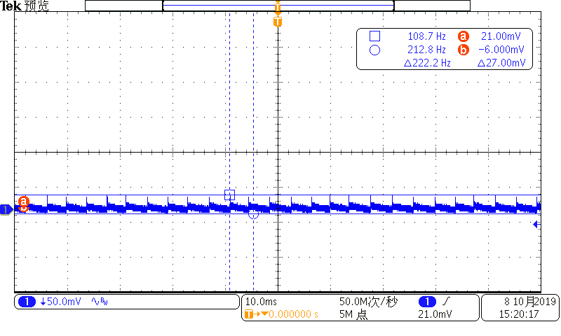
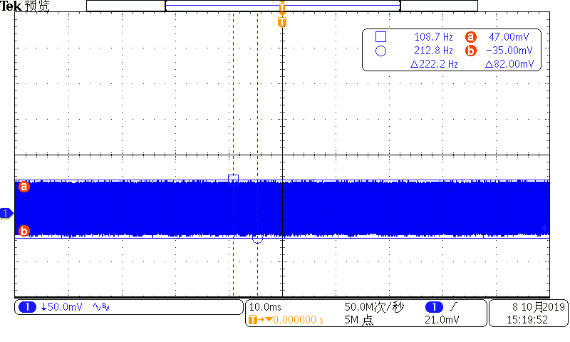
DRAIN(蓝色)端、CS(红色)端波形图:


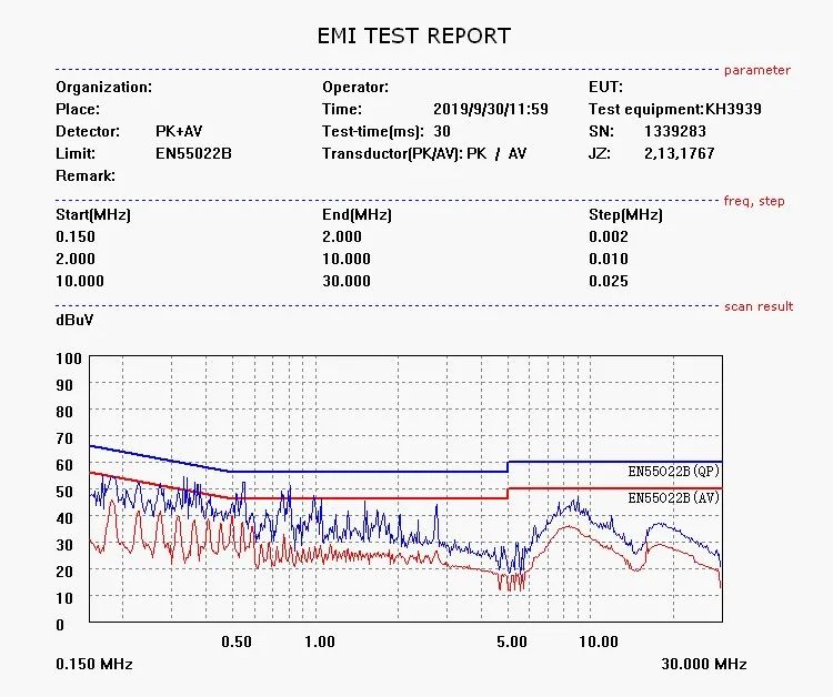
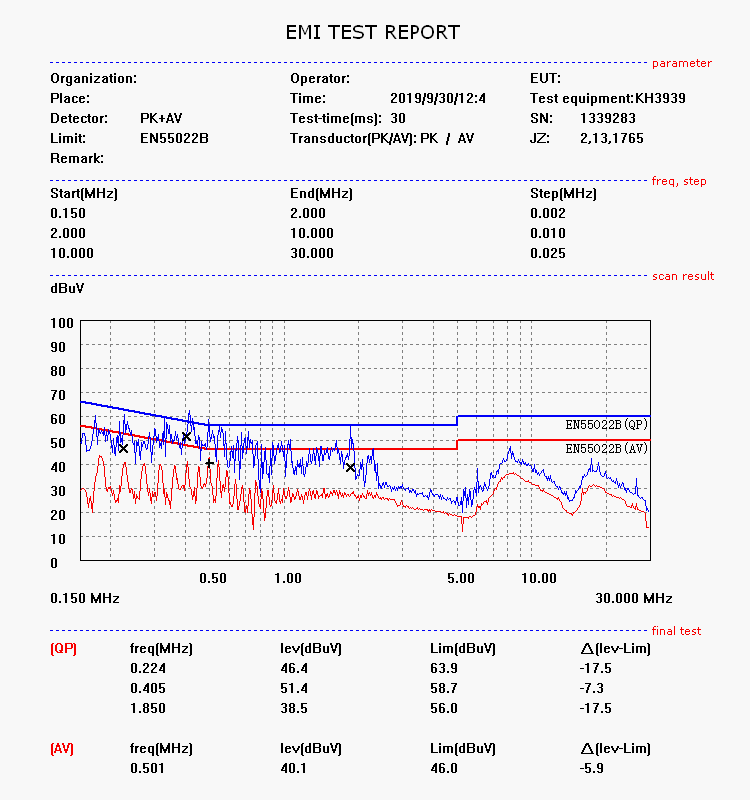
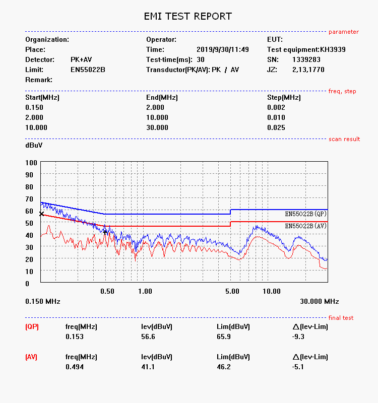
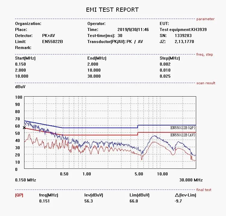
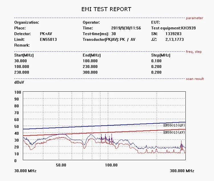
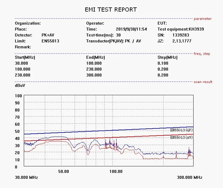
05、EMI 评估测试
测试条件:
输入:AC115V/60Hz@230V/50Hz;
输出负载:功率电阻;
限值标准参考:EN55013、EN55022B。(辐射测试结果仅供参考)
多种方案,欢迎随时交流沟通。思睿达联系人:何工 18923426660,E-mail:manjie@threeda.com,欢迎来电咨询,申请样品。感谢!